
Extreme ultraviolet lithography
Lithography using 13.5 nm UV light
Extreme ultraviolet lithography ▸ Facts ▸ Comments ▸ News ▸ Videos
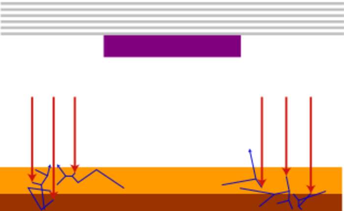
Extreme ultraviolet lithography is a cutting-edge technology used in the semiconductor industry for manufacturing integrated circuits (ICs). It is a type of photolithography that uses extreme ultraviolet (EUV) light to create intricate patterns on silicon wafers.
| 0 shares | ShareTweetSavePostSend |
![Intel’s Chip-Making Unit Posts $7 Billion Operating Loss [Video]](https://video.newsserve.net/300/v/20240403/1371726912-Intel-Chip-Making-Unit-Posts-Billion.jpg) Intel’s Chip-Making Unit Posts $7 Billion Operating Loss Credit: Wibbitz Top Stories Duration: 01:31Published | |
You Might Like
No news matches foundSorry, we were unable to find any results in our database for your queryFree news archive accessDid you know? You are eligible to search our news archive with millions of news references free of charge. To do this, please sign in first at the top of the screen. • Information about free access to our news archive Search this site and the web:  |